





Maximizing Space: Binder Unveils Angled M12 Connectors for Centered PCB Integration

In the rapidly evolving landscape of industrial automation and sensor technology, the drive toward miniaturization remains a dominant force. As devices shrink, the challenge of maintaining robust connectivity within restricted physical envelopes becomes increasingly complex. binder, a global leader in circular connectors, has addressed this engineering hurdle with the introduction of its new line of angled M12 panel-mount connectors specifically designed for centered PCB mounting. By reimagining the interface between the connector and the circuit board, binder is providing design engineers with a critical tool to reduce housing footprints without compromising electrical performance.
The Evolution of M12 Connectivity: Core Facts
The M12 connector has long served as the industry standard for industrial automation, prized for its durability, sealing capabilities, and reliability in harsh environments. However, traditional panel-mount M12 connectors typically sit on top of a printed circuit board (PCB). In compact, tubular sensor housings, this configuration creates a "stacking" effect, where the combined height of the PCB and the connector dictates the minimum diameter of the housing.
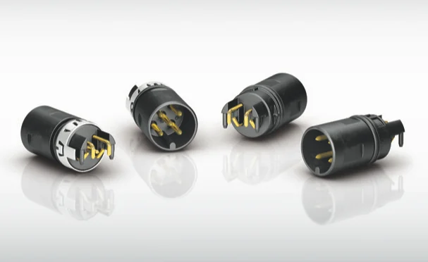
Binder’s latest innovation fundamentally changes this geometry. The new angled M12-A panel-mount connector is engineered to receive the PCB directly at its front edge. Instead of resting on the surface, the connector allows the PCB to slide into the connector body, with contacts extending through the board from both the top and bottom. This aligns the connector’s central axis with the plane of the PCB, effectively neutralizing the "height penalty" associated with traditional surface-mounting.
Key technical specifications of the new product line include:
- Design Orientation: Angled configuration for edge-mounting.
- PCB Compatibility: Optimized for boards with thicknesses ranging from 1 mm to 2 mm.
- Manufacturing Readiness: Utilizes Through-Hole Reflow (THR) technology, making it fully compatible with automated SMT (Surface Mount Technology) assembly lines.
- Assembly Efficiency: Features an integrated pickup surface, allowing standard pick-and-place robotics to handle the components during mass production.
Chronology of the Innovation: From Design to Deployment
The development of this connector series reflects a broader shift in industrial design toward "Smart Sensing." As sensors become more pervasive in robotic arms, diagnostic equipment, and automated process control, the demand for slim, tubular form factors has surged.
- Phase I: Identifying the Bottleneck. Market analysis conducted by binder’s engineering teams identified that many sensor manufacturers were forced to use manual, labor-intensive wiring processes to connect PCBs to panel-mounted interfaces because standard connector footprints were too large for the desired cylindrical housings.
- Phase II: Prototype Development. The engineering objective was clear: create a connector that could be soldered directly to the PCB during the standard reflow oven process, eliminating the need for delicate manual soldering of discrete wires.
- Phase III: Geometry Optimization. By moving the interface point to the edge of the PCB, the design team achieved a centered alignment. This allows the PCB to run through the entire length of a tubular housing, maximizing the usable surface area for electronic components.
- Phase IV: Industrial Validation. Following rigorous testing for mechanical stress, thermal stability in reflow environments, and signal integrity, the connectors were released to satisfy the high-volume requirements of the automation and sensor markets.
Supporting Data and Engineering Implications
The primary advantage of this new design is the reclamation of internal volume. In a traditional setup, if a sensor designer uses a 20mm diameter housing, a significant portion of that diameter is consumed by the vertical clearance required for a top-mounted connector. By utilizing the centered mounting approach, the connector effectively "disappears" into the plane of the PCB.

The Mathematics of Miniaturization
For a design engineer, every millimeter counts. If a standard M12 connector adds 5 to 8 mm of height above the PCB, the housing diameter must accommodate that height plus the width of the PCB. By adopting the edge-mount approach, the "height" of the connector is reduced to the thickness of the PCB itself. This allows for:
- Reduced Housing Diameter: Designers can opt for smaller, more cost-effective tubular housings.
- Increased Component Density: With the connector occupying the edge, the central "real estate" of the PCB is freed for additional processing power, memory, or sensor arrays.
- Improved Structural Integrity: Mounting the connector at the edge of the board, supported by the housing’s panel wall, creates a more rigid assembly capable of withstanding the vibration common in industrial settings.
Official Perspectives: The Value of Reflow Compatibility
A critical component of this release is the adoption of THR (Through-Hole Reflow) technology. In official commentary regarding the release, engineering leads at binder have emphasized that this is not merely a mechanical change, but a manufacturing one.
"For high-volume producers, the bottleneck is often the assembly line," a company representative noted. "Manual soldering is not only slow and prone to human error, but it also introduces inconsistencies in solder joint quality. By engineering the connector to be compatible with standard reflow ovens, we are enabling our customers to integrate the connector into their existing automated workflows. The integrated pickup surface is designed specifically for vacuum-nozzle pick-and-place machines, ensuring that the connector is treated just like any other passive or active component on the board."
This transition from manual assembly to automated production represents a significant reduction in Total Cost of Ownership (TCO). By eliminating secondary assembly steps, manufacturers can increase their throughput, reduce labor costs, and achieve a higher level of statistical process control over their final products.
Implications for Future Industrial Design
The introduction of the angled M12 connector has wide-reaching implications for several sectors, most notably in the fields of robotics, medical devices, and smart infrastructure.
Robotics and Collaborative Systems
As cobots (collaborative robots) become smaller and more mobile, the cables and connectors integrated into their joints must be as compact as possible. The centered PCB mounting allows for a "clean" cable exit that aligns with the axis of rotation, reducing cable fatigue and preventing snagging during complex movements.

Medical Diagnostic Equipment
In handheld diagnostic devices, where ergonomics and weight are paramount, the ability to fit a high-speed, reliable M12 interface into a slim, hand-held housing allows for more sophisticated sensors to be integrated into portable tools. The robustness of the M12 standard ensures these devices can be sterilized or cleaned without risking the integrity of the internal electronics.
The Standardized Future
By providing a standardized M12 interface in a form factor that behaves like an SMT component, binder is helping to bridge the gap between heavy-duty industrial hardware and the compact world of consumer-grade electronics. This versatility ensures that as the "Industrial Internet of Things" (IIoT) continues to expand, engineers have the components necessary to create hardware that is both rugged and highly integrated.
Conclusion: A Strategic Sourcing Option
Binder’s decision to expand its M12 product range with these angled connectors is a calculated move to capture the growing segment of the market focused on ultra-compact sensor housings. As manufacturers continue to push the boundaries of what can be packed into a cylindrical enclosure, the ability to optimize space through component architecture becomes a competitive advantage.
For engineers and procurement professionals, these connectors offer more than just a new design—they offer a pathway to more efficient manufacturing. By aligning the electrical interface with the mechanical axis of the device, binder has simplified the assembly process while enhancing the potential for performance. As industries shift toward increasingly automated and miniaturized solutions, the relevance of such specialized, high-reliability components will only continue to grow, providing a standardized, scalable solution for the complex connectivity challenges of tomorrow.
For those interested in integrating this technology into their upcoming designs, full technical documentation, CAD models, and compatibility matrices are available through the binder official portal, reflecting the company’s ongoing commitment to supporting the global engineering community through accessible and innovative connectivity solutions.