


The Silicon Photonics Pivot: STMicroelectronics and the Industrialization of AI Connectivity

As artificial intelligence clusters evolve from simple racks of servers into sprawling, interconnected "AI factories" housing thousands of high-performance accelerators, the traditional constraints of copper cabling have reached a breaking point. In the high-stakes race to build the next generation of data center infrastructure, compute power is no longer the only bottleneck—data movement is.
To overcome the inherent physical limitations of electrical signaling, the industry is increasingly turning to silicon photonics. By integrating optical interconnects directly into the compute fabric, data centers can achieve the bandwidth, reach, and power efficiency required for the AI era. However, moving from experimental prototypes to mass-scale deployment remains a formidable hurdle. STMicroelectronics (ST) is positioning itself at the epicenter of this shift, betting that the future of photonics will be defined not just by raw performance, but by the ability to industrialize production at scale.
The Limits of Copper: Why Photonics is Essential
For decades, copper has served as the workhorse of data center connectivity. Yet, as bandwidth requirements surge to meet the demands of large language models and real-time inference, copper has hit a wall. Electrical signals over copper suffer from severe signal degradation at high frequencies and over long distances, forcing the use of power-hungry re-timers and signal conditioners that add latency and heat.

As Sylvie Gellida, general manager of ST’s Optical and RF Foundry Division, points out, AI data centers are starving for more routing capability within the rack and higher bandwidth density between system elements. "Copper increasingly constrains both," she notes. Optical links provide a superior alternative, offering extended reach, lower power consumption, and the ability to pack more data-carrying capacity into a smaller physical footprint.
The industry roadmap currently favors a phased migration: starting with pluggable optical transceivers, moving toward near-packaged optics (NPO) that bring the optical engine closer to the ASIC, and eventually achieving co-packaged optics (CPO), where the photonic and electronic dies are integrated within the same package. Achieving this transition requires a mastery of packaging, thermal management, and, crucially, high-volume manufacturing.
A Chronology of ST’s Photonics Journey
ST’s reentry into the silicon photonics market is the result of a decade-long strategic persistence. The company first entered the space nearly ten years ago with its "PIC25" platform, which supported 25-GBaud signaling for 50G-per-lane applications.

While the technology was sound, the market was not. "The killer application wasn’t there," Gellida explains. "ST put the business activity on hold, but not the R&D, because we believed the application would eventually come."
During that hiatus, ST continued to refine its intellectual property, waiting for the inflection point where AI demand would align with its manufacturing capabilities. Today, that alignment is clear. With the launch of the PIC100 platform—supporting 100-GBaud signaling for 200G-per-lane applications—ST is ramping production on 300-mm wafers. By leveraging its established CMOS manufacturing infrastructure, ST is transforming photonics from a boutique, low-yield specialty into a standardized, high-volume semiconductor product.
Supporting Data: Scaling on 300-mm Wafers
The primary differentiator for ST is its commitment to 300-mm wafer manufacturing. In the world of semiconductor foundries, transitioning from 200-mm to 300-mm is the benchmark for achieving the economies of scale necessary to support global hyperscalers.

"Today we’re supplying silicon photonics wafers in Crolles, France, on 300-mm wafers," Gellida states. "For the volumes required by AI data centers and AI factories, 300-mm manufacturing brings together tools, accuracy, volume, and yield."
By utilizing its proven CMOS-like process, ST is achieving yields that significantly outpace traditional photonics manufacturing, which has historically relied on smaller wafer sizes and more manual assembly processes. This industrial-grade reliability is critical for customers—primarily transceiver module makers and PIC design houses—who need assurance that their optical engines can be produced in the millions without defect spikes.
The Sicoya Proof Point: 1.6T Operation
A tangible validation of ST’s platform strategy can be seen in the recent collaboration with Sicoya, a Berlin-based innovator in silicon photonics. At the Optical Fiber Communication Conference (OFC) earlier this year, the two companies demonstrated a 1.6T OSFP module utilizing the PIC100 platform.

The module, which targets scale-out networks, runs eight lanes at 200G per lane. The design represents a masterclass in modern chip integration:
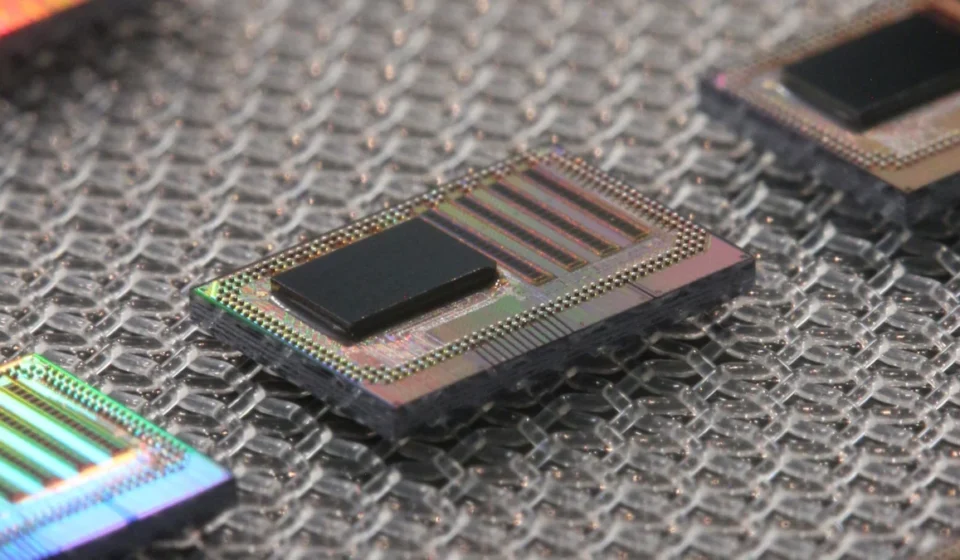
- Die Stacking: Sicoya utilized die-stacking to place the transimpedance amplifier (TIA) directly on top of the photonic integrated circuit (PIC).
- Performance Optimization: This physical proximity allows for extremely short RF paths between the photodiodes and the amplifier, minimizing parasitics and enhancing signal integrity.
- Internal Control Loops: The design incorporates advanced features like integrated variable optical attenuators, which are managed by the TIA itself. This eliminates the need for an external microcontroller to handle power-level adjustments, reducing complexity and power overhead for the module manufacturer.
Hanjo Rhee, CTO of Sicoya, emphasizes that this is not just a laboratory success but a scalable industrial solution. "The demo proved that these more complex photonic products for these pluggables are possible and that they are possible with ST’s platform," Rhee said.
Sicoya’s transition from building entire modules to focusing on chip-level integration—supported by a high-volume foundry like ST—highlights a broader trend: the industry is moving away from monolithic, bespoke designs toward a modular ecosystem where foundries provide the "building blocks" (PICs, EICs, and packaging) for designers to assemble.

Implications for the Future of Data Centers
The shift toward silicon photonics carries profound implications for the future of hardware design. As ST expands its offerings to include through-silicon vias (TSVs), bumping, and advanced packaging, it is effectively becoming a "one-stop shop" for optical interconnects.
1. The Death of the DSP?
One of the most exciting implications of moving optics closer to the switch ASIC or GPU is the potential to eliminate the need for digital signal processors (DSPs) in certain short-reach applications. Because shorter electrical paths reduce the need for aggressive retiming, the power savings could be immense. However, this relies entirely on the successful deployment of NPO and CPO technologies.
2. The Packaging Challenge
While the photonic and electronic chips are ready for mass production, the assembly remains the "hard part." Soldering an optical engine directly to a main board poses significant challenges, particularly regarding thermal expansion and the survivability of optical connectors during reflow soldering. The industry is currently racing to develop detachable optical connectors that can withstand high-heat manufacturing processes—a requirement for the mass adoption of co-packaged optics.

3. A New Model of Serviceability
As optics move closer to the compute core, the industry must rethink how systems are serviced. If an optical engine is integrated within a GPU package, it cannot be replaced like a traditional pluggable transceiver. This is forcing designers to rethink system architecture, with some looking toward "optical tiles" or modular assemblies that can be replaced without discarding an entire multi-thousand-dollar accelerator board.
Conclusion: The Industrialization Mandate
The AI revolution is driving a fundamental change in the hierarchy of data center needs. While the industry spent the last decade obsessed with transistor density, the next decade will be defined by the efficiency of data movement.
STMicroelectronics’ return to the silicon photonics market is timely. By treating photonics not as a niche laboratory experiment, but as a standard semiconductor component that can be manufactured on 300-mm wafers, ST is addressing the core concern of the hyperscalers: reliability and volume. Whether it is through Sicoya’s die-stacked transceivers or the eventual integration of CPO into future AI servers, the path forward is clear. The winners in the silicon photonics space will not necessarily be those with the most exotic light-manipulation techniques, but those who can successfully navigate the brutal, unforgiving reality of industrial-scale manufacturing. As the AI infrastructure landscape continues to evolve, ST’s "one-stop shop" approach may prove to be the linchpin that finally brings the promise of photonics to the heart of the data center.